


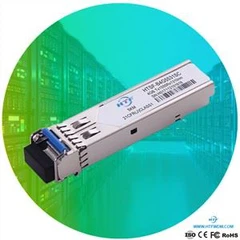


400G QSFP56-DD Transceiver
Up to 53.125Gbps data rate per channel by
PAM4 modulation
Support 400GAUI-8 electrical interface
Integrated 850nm VCSEL array and PD array
Single MPO16 connector receptacle optical
interface compliant
DDM function implemented
Hot-pluggable QSFP-DD form factor
Maximum power consumption 8W
Single +3.3V power supply
Reach up to 70m on MMF(OM3)
Reach up to 100m on MMF(OM4)
Compliant with ROHS2.0
|
Pad |
L gic |
S nbol |
Description |
Plug Sequeηceq |
Notes |
|
||
|
1 |
|
GND |
Ground |
lB |
1 |
|
||
|
2 |
CML |
Tx2n |
Transmitter Inverted Data I put |
3B |
|
|
||
|
3 |
CML-I |
Tx2p |
Transmitter Non -Inverted Data Input |
3B |
|
|
||
|
4 |
|
GND |
Ground |
lB |
1 |
|
||
|
5 |
CML-I |
Tx4n |
Transmitter Inverted Data Input |
3B |
|
|
||
|
6 |
CML-I |
Tx4p |
Transmitter Non -Inverted Data Input |
3B |
|
|
||
|
7 |
|
GND |
Ground |
lB |
1 |
|
||
|
8 |
LVTTL -I |
ModSelL |
Module Select |
3B |
|
|
||
|
9 |
LVTTL -I |
ResetL |
Modul e Reset |
3B |
|
|
||
|
10 |
|
VccRx |
+3 .3V Power suppl y Receiver |
2B |
2 |
|
||
|
11 |
LVCMOS - 0 |
SCL |
2 -wire seria l interface clock |
3B |
|
|
||
|
12 |
LVCMOS - O |
SDA |
2 -wire seri al interface data |
3B |
|
|
||
|
13 |
|
GND |
Ground |
lB |
1 |
|
||
|
14 |
CML-0 |
Rx3p |
Receiver Non-In verted Data Output |
3B |
|
|
||
|
15 |
CML-0 |
Rx3n |
Receiver Inverted Data Output |
3B |
|
|
||
|
16 |
|
GND |
Ground |
lB |
1 |
|
||
|
17 |
CML-0 |
Rxlp |
Receiver Non -Inverted Data Output |
3B |
|
|
||
|
18 |
CML-0 |
Rxln |
Receiver Inverted Data Output |
3B |
|
|
||
|
19 |
|
GND |
Ground |
1B |
1 |
|
||
|
20 |
|
GND |
Ground |
1B |
1 |
|
||
|
21 |
CML-0 |
Rx2n |
Receiver Inverted Data Output |
3B |
|
|
||
|
22 |
CML-0 |
Rx2p |
Receiver Non -Inverted Data output |
3B |
|
|
||
|
23 |
|
GND |
Ground |
lB |
1 |
|
||
|
24 |
CML-0 |
Rx4n |
Receiver Inverted Data Output |
3B |
|
|
||
|
25 |
CML-0 |
Rx4p |
Receiver Non -Inverted Data Output. |
3B |
|
|
||
|
26 |
|
GND |
Ground |
lB |
1 |
|
||
|
27 |
LVTTL -0 |
Mod PrsL |
Module Present |
3B |
|
|
||
|
28 |
LVTTL-0 |
IntL |
Interrupt |
3B |
|
|
||
|
29 |
|
VccTx |
+3 . 3V Power supply transmitter |
2B |
2 |
|
||
|
30 |
|
Vccl |
+3 .3V Power supply |
2B |
2 |
|
||
|
31 |
LVTTL-I |
LPMode |
Low Power mode; |
3B |
|
|
||
|
32 |
|
GND |
Ground |
1B |
1 |
|
||
|
33 |
CML-I |
Tx3p |
Transmitter Non -Inve rted Data Input |
3B |
|
|
||
|
34 |
CML-I |
Tx3n |
Transmitter Inverted Data Input |
3B |
|
|
||
|
35 |
|
GND |
Ground |
lB |
1 |
|
||
|
36 |
CML-I |
Txlp |
Tran sm tter Non -Inverted Data Input |
3B |
|
|
||
|
37 |
CML-I |
Txln |
Transmitter Inverted Data I put |
3B |
|
|
||
|
38 |
|
GND |
Ground |
lB |
1 |
|
||
|
|
39 |
|
GND |
Gr und |
lA |
1 |
||
|
|
40 |
CML-I |
Tx6n |
Transmitter Inverted Data Input |
3A |
|
||
|
|
41 |
CML-I |
Tx6p |
Transmitter Non -Inverted Data Input |
3A |
|
||
|
|
42 |
|
GND |
Ground |
lA |
1 |
||
|
|
43 |
CML-I |
Tx8n |
Transmitter Inverted Data Input |
3A |
|
||
|
|
44 |
CML-I |
Tx8p |
Transmitter Non-Inverted Data Input |
3A |
|
||
|
|
45 |
|
GND |
Ground |
lA |
1 |
||
|
|
46 |
|
Reserved |
For future use |
3A |
3 |
||
|
|
47 |
|
VSl |
dule Vendor Specific 1 |
3A |
3 |
||
|
|
48 |
|
VccRxl |
3.3V Power Supply |
2A |
2 |
||
|
|
49 |
|
VS2 |
Module Vendor Specific 2 |
3A |
3 |
||
|
|
50 |
|
VS3 |
Module Vendor Specific 3 |
3A |
3 |
||
|
|
51 |
|
GND |
Ground |
lA |
1 |
||
|
|
52 |
CML-0 |
Rx7p |
Rece ver Non-Inverted Data Output |
3A |
|
||
|
|
53 |
CML-0 |
Rx7n |
Receiver Inverted Data Output |
3A |
|
||
|
|
54 |
|
GND |
Ground |
lA |
1 |
||
|
|
55 |
CML-0 |
Rx5p |
Receiver Non-Inverted Data Output |
3A |
|
||
|
|
56 |
CML-0 |
Rx5n |
Receiver Inverted Data Output |
3A |
|
||
|
|
57 |
|
GND |
Gr und |
lA |
1 |
||
|
|
58 |
|
GND |
Gr und |
lA |
1 |
||
|
|
59 |
CML-0 |
Rx6n |
Receiver nverted Data Output |
3A |
|
||
|
|
60 |
CML-0 |
Rx6p |
Receiver Non-Inverted Data Output |
3A |
|
||
|
|
61 |
|
GND |
Ground |
lA |
1 |
||
|
|
62 |
CML-0 |
Rx8n |
Receiver Inverted Data Output |
3A |
|
||
|
|
63 |
CML 0 |
Rx8p |
Receiver Non -Inverted Data Output |
3A |
|
||
|
|
64 |
|
GND |
Ground |
lA |
1 |
||
|
|
65 |
|
NC |
No Connect |
3A |
3 |
||
|
|
66 |
|
Reserved |
For future use |
3A |
3 |
||
|
|
67 |
|
VccTxl |
3.3V p wer supply |
2A |
2 |
||
|
|
68 |
|
Vcc2 |
3.3V p wer Supply |
2A |
2 |
||
|
|
69 |
LVTTL-I |
ePPS |
Precision Time Protocol (PTP) reference clock input |
3A |
3 |
||
|
|
70 |
|
GND |
Ground |
lA |
1 |
||
|
|
71 |
CML-I |
Tx7p |
Transmitter Non -Inverted Data Input |
3A |
|
||
|
|
72 |
CML-I |
Tx7n |
Transmitter Inverted Data Input |
3A |
|
||
|
|
73 |
|
GND |
Gr und |
lA |
1 |
||
|
|
74 |
CML-I |
Tx5p |
Transmitter Non nverted Data Input |
3A |
|
||
|
|
75 |
CML-I |
Tx5n |
Transmitter Inverted Data Input |
3A |
|
||
|
|
76 |
|
GND |
Ground |
lA |
1 |
||
|
|
Note 1: QSFP-DD uses common ground (GND)for all signals and supply (power). All are common within the QSFP-DD module and all module voltages are referenced to this potent ial unless otherwise noted . Connect these directly to the host board signal- common gr und plane . Note 2: VccRx , VccRxl, Vccl, Vcc2, VccTx and VccTxl shall be applied concurrently . Requirements defined for the host side of the Host Card Edge Connect r are listed in Table 7. VccRx , VccRxl , Vccl , Vcc2 , VccTx and VccTxl may be internally connected within the module in any combination . The connector Vcc pi s are each rated for a maximum current of 1000 mA . Note 3: All Vend r Specific , Reserved , N Connect and ePPS (if n t used) pins may be terminated with 50 Ohms to ground on the h st. Pad 65 (No Connect) shall be left unconnected within the module . Vend r specific and Reserved pads shall have an impedance to GND that is greater than 10 kOhms and less than 100 pF . Note 4: Plug Sequence specifies the mating sequence of the host connector and module. The sequence is lA, 2A, 3A, lB, 2B, 3B. (see Figure 2 f r pad l cations) contact sequence A will make, then break c ntact with add tional QSFP-DD pads . Sequence lA,lB will then occur simultaneously , followed by 2A,2B,followed by 3A,3B . |
|||||||
Hot Tags: dwdm power meter 400g qsfp56-dd transceiver, China, manufacturers, suppliers, factory, customized, buy, price, bulk, compatible brand, Dwdm Power Meter 400G QSFP56 DD Transceiver, 400G QSFP DD LR 10km Optic Module, 400G QSFP DD ER4 40km Optic Module
