


There are more and more voices in the industry talking about what future optical modules will look like, the architecture of switches, and the shape of devices. There was even a panel discussion on the OFC for three years in a row, 18, 19, 20, all of which was, will the pluggable optical module be scrapped? When to scrap?
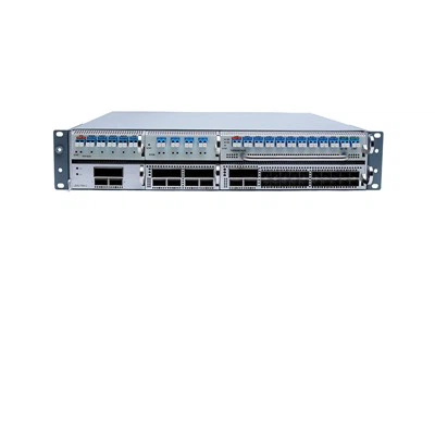
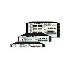
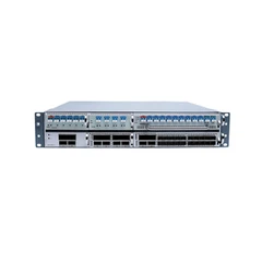
A) The current mode of interconnect between optical modules and devices will definitely be replaced, as the maximum density of the current switch is 32 400G optical modules on 1RU with the corresponding capacity of 12.8t. The capacity of data center switches doubles every two years, and after two or three years there is demand for 51.2t. Assuming that the 800G optical module is mature and the size of power consumption is small enough, the switch can be doubled, then the maximum under 2RU can provide 51.2Tb capacity, but it is almost impossible to continue to improve, at least based on the current pluggable module path is impossible.
B) The market demand for post-optical module technology should appear around 2024. There are two reasons. One is that the bottleneck of switch capacity reaching 51.2t will be highlighted around 2024. The other is that the demand for optical modules in Ethernet data center is predicted to decline in 2026.
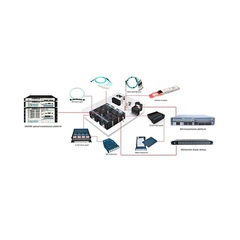
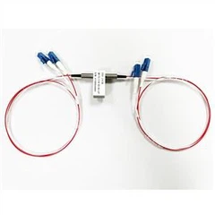
C) The two most competitive solutions in the post-optical module era are on-board optical OBO and co-packaged optical CPO. Among them, the optical module scheme, the front panel is a high-speed electrical port, the optical module and the exchange chip between a long PCB wiring; the on-board optical OBO scheme directly places the optical module on the main board inside the switch. The panel only has a light port, so the width is higher, the power consumption is easier to control, the high-speed PCB wiring is shortened, and the signal integrity is better. Total package CPO directly encapsulates the optical engine (transceiver module) and the electrical switching chip into a chip on the same substrate, which can solve the heat dissipation problem and save a lot of SerDes functions and power consumption.
D) Further, the total packaging CPO scheme may also be divided into two phases. The initial phase consists of 2.5d packaging of electrical components and optical devices on a layer of medium to form a multi-chip module (MCM). The ultimate goal is to achieve 3D packaging through the silicon through hole, in the real sense of a single optical, electrical chip packaging.
E) How much power can OBO and CPO save? Obviously, due to the simplification of SerDes and the elimination of CDR,DFE/CTLE/FFE and other functions, CPO still has a significant power consumption advantage over OBO, and OBO also has some power consumption reduction on the basis of pluggable modules, mainly for the elimination of DFE and shorter PCB wiring without strong equilibrium. Compared with MCM, TSV has no obvious advantage in power consumption. Considering the difficulty of total packaging, it is not bad to be able to make a 2.5d MCM.
F) Although both OBO and CPO have corresponding industry alliances, this new technology still faces some challenges, at least in terms of heat dissipation.
The new technology may not be ready for large-scale commercial use right away, but it may not be far off. While OBO or CPO won't replace the existing pluggable optical modules immediately in the next five to eight years, it's likely that in three or four years the trend will start to take over. Although 10 years will not be in the form of a kind of entirely in the hands of the line card, there is a pluggable to board to MCM or TSV encapsulation of transition process, for equipment business, the early preparation is necessary, this revolutionary technology can largely change the configuration of communication equipment and industrial chain.